
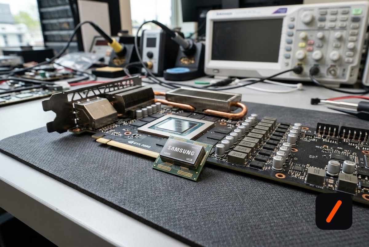
Samsung has shipped the industry's first 12-layer HBM4E memory samples, running at up to 16 Gbps per pin and delivering roughly 3.6 TB/s of bandwidth per stack at 48GB capacity. That is the memory that decides how fast the next wave of AI accelerators can actually run, and being first to sample it puts Samsung back in a fight it had been losing to SK hynix.
- Samsung's HBM4E samples run at a 14 Gbps baseline and up to 16 Gbps per pin, well above the JEDEC HBM4 floor.
- Each 12-high stack delivers about 3.6 TB/s of bandwidth at 48GB, feeding data to GPUs faster than any shipping memory.
- HBM, not raw compute, is the real bottleneck for large AI models, so memory bandwidth increasingly sets accelerator performance.
- The move reopens a three-way race with SK hynix and Micron to supply memory for chips like NVIDIA's Vera Rubin and AMD's Instinct line.
What did Samsung announce?
Samsung has begun sampling HBM4E built as a 12-high stack, meaning twelve DRAM dies stacked vertically on a logic base and wired together with thousands of through-silicon vias. The samples run at a 14 Gbps baseline per pin and up to 16 Gbps, yielding around 3.6 TB/s of bandwidth per stack at 48GB of capacity. Sampling is not mass production, but it is the milestone that lets accelerator makers begin qualifying the parts for their next platforms, and being first to hand out working silicon matters in a market where design wins are locked in years ahead.
RelatedSK hynix and Samsung Race to Ship 12-Layer HBM4E
Why is memory the real AI bottleneck?
Modern accelerators are rarely limited by how many math operations they can do. They are limited by how fast they can feed data to those math units. A large language model has to stream billions of parameters through the chip for every token it generates, and if the memory cannot supply them quickly enough, the expensive compute cores sit idle waiting. That is why bandwidth, measured in terabytes per second, has become the headline spec. Every generation of HBM that widens the pipe directly raises the ceiling on model size and inference speed, which is why the memory roadmap now drives the accelerator roadmap rather than the other way around.
| Spec | HBM3E | HBM4 | HBM4E (Samsung sample) |
|---|---|---|---|
| Per-pin speed | ~9.6 Gbps | ~8 Gbps (wider bus) | 14 Gbps, up to 16 |
| Bandwidth per stack | ~1.2 TB/s | ~2.0 TB/s | ~3.6 TB/s |
| Stack height | 8-12 high | 12-16 high | 12 high |
| Capacity | 24-36GB | 36-48GB | 48GB |
| Status | Shipping | Ramping | Sampling |
What does HBM4E change versus HBM4?
HBM4 already widened the interface to a 2,048-bit bus, roughly doubling effective bandwidth over HBM3E even at modest per-pin speeds. HBM4E is the performance-extended follow-on: it pushes per-pin data rates higher, and Samsung's samples clearing 14 to 16 Gbps translate into that roughly 3.6 TB/s figure per stack. Multiply that across the eight or more stacks that surround a flagship GPU and the total memory bandwidth reaches into the tens of terabytes per second, which is what makes trillion-parameter inference practical rather than theoretical. The capacity bump to 48GB per stack also lets a single accelerator hold more of a model locally, cutting the slow trips to system memory.
Who else is in this race?
Memory is now a three-way contest. SK hynix has led the HBM3E and HBM4 era and signed a multi-year partnership with NVIDIA to co-develop memory for its Vera Rubin, Vera CPU, RTX Spark and Jetson Thor platforms. Micron has closed much of the gap. Samsung, which stumbled on HBM3E qualification, is using HBM4E to try to leapfrog back to the front. On the buyer side, Samsung is also supplying HBM4 for AMD's Instinct MI455X, so the same memory war plays out across both major GPU camps. Whoever qualifies fastest at the highest yield captures the most valuable sockets in the industry.
RelatedHBM4 Enters Production for NVIDIA's Vera Rubin
- Qualification, not samples. The real win is passing an accelerator maker's qualification and shipping in volume, which is where Samsung faltered on HBM3E.
- Yield at 12-high. Stacking twelve dies with reliable through-silicon vias is hard. Yield decides margins and supply.
- Design-win split. Watch how NVIDIA and AMD divide HBM4E orders across Samsung, SK hynix and Micron.
- Thermals. Faster, taller stacks run hotter. Cooling and power delivery become the next constraint.
Our take
It is easy to scroll past a memory sampling announcement, but this is one of the most consequential hardware stories of the year. The AI buildout is fundamentally bandwidth-bound, and HBM4E at 3.6 TB/s per stack raises the ceiling on what a single accelerator can do. For Samsung, being first to sample 12-high HBM4E is a credible shot at reclaiming leadership it lost during the HBM3E generation. The caveat is real: sampling is the easy part, and mass-production yield on a twelve-die stack is where fortunes are actually won. But the direction of travel is clear, and memory, not compute, is where the next round of AI performance will be decided.
- OfficialSamsung Semiconductor - HBM HBM product line and specs
- ReferenceJEDEC HBM4 standard the interface spec HBM4E extends
- ReferenceFuture hardware tracker accelerator and memory roadmap
Original analysis by GenZTech. Specifications reflect Samsung's sampled HBM4E parts as of July 2026.