
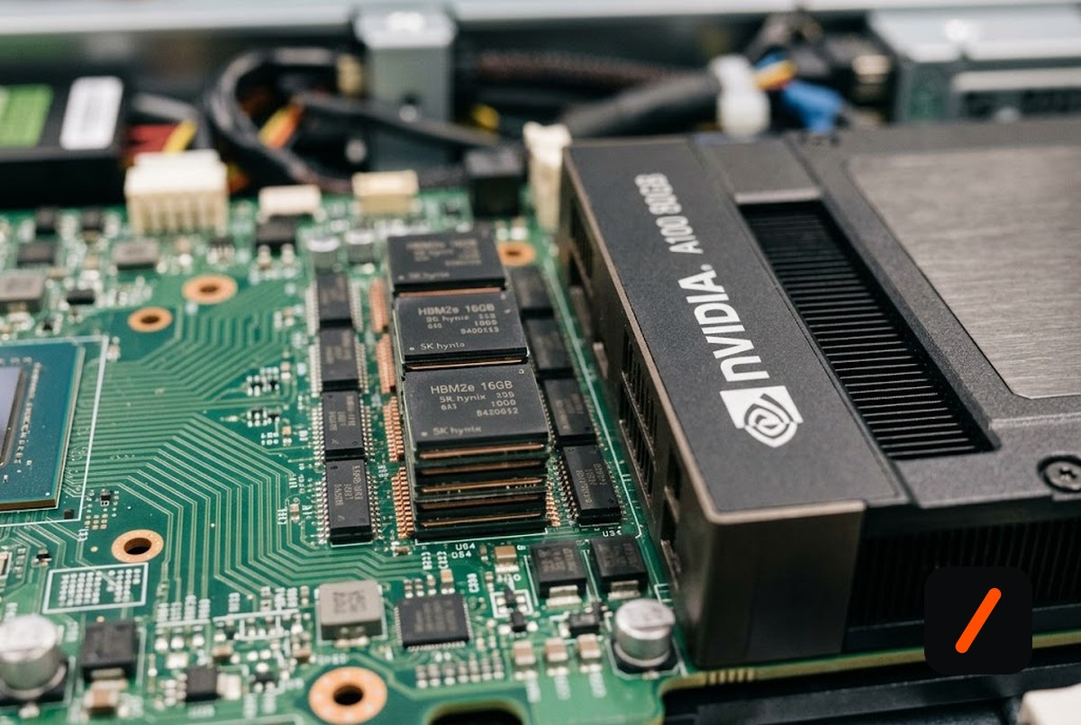
Nvidia has told all three big memory makers it wants 16-high HBM4 stacks in the second half of 2026, and that single request has set off a manufacturing sprint at SK Hynix, Samsung and Micron. Sixteen-layer HBM has never been commercialized, and the reason is physical: to stack that many DRAM dies inside the same package height, each wafer has to be thinned to roughly 30 microns, down from about 50, without cracking or warping. Our take is that this is the real bottleneck of the AI buildout right now. GPUs are abundant relative to the exotic memory that feeds them, so whoever masters 16-Hi first effectively rations the frontier.
- Nvidia requested 16-high HBM4 delivery by Q4 2026 for its next-generation Rubin platform, a stack height no supplier has shipped before.
- The engineering wall is wafer thinning: 16 layers in the same z-height means ~30 micron dies, with severe warpage and thermal risk.
- SK Hynix leads HBM at roughly 50-55% share and completed the first HBM4 development; Samsung and Micron are sprinting to close the gap.
- HBM4 speeds hit about 11 Gbps per pin with total bandwidth above 2.8 TB/s, and SK Hynix is pairing DRAM with a TSMC-built logic base die.
What did Nvidia actually ask for?
Nvidia requested 16-Hi HBM4 samples and a supply path to volume by the fourth quarter, tied to its Rubin generation of accelerators. Both SK Hynix and Samsung have already handed Nvidia paid final HBM4 samples, which is the industry signal that talks have moved from engineering to commercial negotiation. The jump from 12-high to 16-high is not a marketing number; it is a third more capacity and bandwidth in the same footprint next to the GPU, which is exactly what larger models and longer context windows are starving for.
RelatedSK Hynix HBM4 Warning Triggers Record Memory-Stock Selloff
Why is 16-high so hard to build?
Stacking is a game of vertical budget. The package can only be so tall, so adding layers means each DRAM die must get thinner. Existing 12-high parts use wafers around 50 microns thick. Sixteen layers forces that down toward 30 microns, at which point wafers behave like foil: they warp during bonding, trap heat, and fail yield tests. Suppliers are leaning on hybrid bonding and new base-die designs, with SK Hynix using a logic base die fabricated on TSMC's 12nm process, to keep signal integrity and cooling under control. Every micron of thinning is a fresh yield problem.
What does it mean for the market?
The signal for investors is that memory, not logic, is the choke point of the AI trade, and the pricing power sits with the supplier who ships 16-Hi at yield. SK Hynix (KRX: 000660) is the incumbent to beat, with analysts modeling a dominant share of HBM4 for Rubin. Samsung (KRX: 005930) is fighting to reclaim ground after ceding the HBM3E lead, and Micron (NASDAQ: MU) has pivoted hard toward AI data-center memory, even exiting parts of the consumer market. Nvidia (NASDAQ: NVDA) benefits from three-way competition keeping supply flowing, but a stumble at any one vendor tightens the whole Rubin ramp. The number to watch is 16-Hi yield, because that, not headline bandwidth, decides who prices the boom.
| Metric | 12-Hi HBM4 | 16-Hi HBM4 |
|---|---|---|
| Layers | 12 | 16 |
| Wafer thickness | ~50 microns | ~30 microns |
| Status | Sampling and ramping | Development sprint |
| Target | Shipping 2026 | Nvidia asks Q4 2026 |
| Main risk | Base-die logic | Warpage and thermals |
Who is affected?
Hyperscalers and AI labs feel it as availability and cost of the next GPU generation. Cloud renters feel it as the price of an H-class or Rubin instance. And the memory makers feel it as a once-in-a-cycle chance to lock multi-year Nvidia contracts. A class-action suit already alleges the three suppliers inflated memory prices, a reminder that a concentrated market with this much leverage draws scrutiny.
RelatedRAMpocalypse: DRAM Prices Jump 90% as AI Eats Supply
How does this connect to the memory shortage?
The 16-Hi race does not happen in a vacuum. The same AI demand that has Nvidia asking for denser stacks has also sent conventional DRAM prices sharply higher, because every wafer a supplier pours into high-margin HBM is a wafer not making commodity memory. That is why phone makers are quietly warning about component costs and trimming launch lineups this year. HBM is simply more profitable, so the industry's best capacity flows there, and the rest of the market pays the difference. For the memory makers, this is the whole game: HBM3E remains the workhorse and will account for roughly two-thirds of HBM shipments in 2026, while HBM4 and eventually 16-Hi ramp on top. The broader semiconductor market is forecast to grow more than 25% this year toward roughly $975 billion, with memory growing faster than that. The 16-Hi sprint is the leading edge of a supercycle whose second-order effect is a squeeze on everything downstream that also needs DRAM.
- Yield reports. Any credible 16-Hi yield number changes the pecking order overnight.
- Rubin schedule. If HBM slips, the Rubin ramp slips with it, regardless of GPU readiness.
- Second sourcing. Nvidia asking all three vendors is deliberate; watch who actually qualifies for volume.
- OfficialSK Hynix newsroom: HBM4 development and outlook supplier primary
- ReferenceDigiTimes: HBM4 and 16-Hi supply reporting supply-chain reporting
Original analysis by GenZTech. Primary source: SK Hynix Newsroom.