
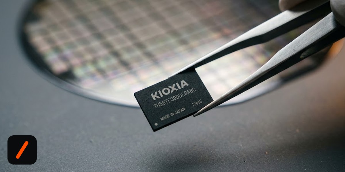
Kioxia and SanDisk introduced a 9th-generation 2Tb QLC 3D flash memory technology on August 12, aimed squarely at AI infrastructure. The specifications that matter: a NAND interface speed of 4.8 Gb/s, a 33% improvement over the previous generation, and bit density above 37 Gb/mm², up to 60% denser than their 8th-generation part. Both numbers point at the same problem, which is that AI data pipelines have started to starve on storage rather than compute.
Why QLC, and why now?
QLC stores four bits per cell. That is the densest mainstream NAND configuration, and historically it came with a reputation problem. More bits per cell means more voltage states packed into the same physical window, which means slower writes, less endurance, and more error correction overhead. For years the standard advice was that QLC belonged in read-heavy, cost-sensitive tiers and nowhere near performance-critical work.
RelatedHuawei, Cambricon Hike AI Chip Prices as HBM Squeeze Bites
AI workloads scrambled that logic. Training and inference pipelines read enormous datasets repeatedly and write comparatively little. That access pattern is close to ideal for QLC: the weakness is write performance and endurance, and the demand is overwhelmingly reads at scale. What was blocking adoption was not the cell type. It was that the surrounding architecture had not caught up.
What CBA and six planes actually do
Two architectural choices carry most of the improvement, and they are worth separating because they solve different bottlenecks.
CBA stands for CMOS directly Bonded to Array. In a conventional 3D NAND die, the control logic sits under or beside the memory array on the same wafer, which forces a compromise: the process that is good for dense memory cells is not the process that is good for fast logic. CBA fabricates the two on separate wafers, each optimized for its own job, and bonds them. The array gets a memory-tuned process, the CMOS gets a logic-tuned one, and the interface between them becomes a manufacturing step rather than a design constraint. That is where the density headroom comes from, and it is also why the companies frame this as more capital-efficient manufacturing: you can improve one side without respinning the other.
The six-plane design addresses throughput instead. A plane is an independently operable subdivision of the die. More planes means more operations proceeding in parallel, so bandwidth rises without the interface having to clock faster. Combined with the 4.8 Gb/s interface, that is what produces the higher read and write bandwidth the companies claim, along with better power efficiency per operation.
The reason this pairing is notable: density and speed usually trade against each other. Packing more bits into a cell typically slows it down. Getting 60% more density and a 33% faster interface in the same generation means the gains came from restructuring the die, not from pushing the cells harder.
Who does this actually help?
Anyone whose AI infrastructure spends real money keeping datasets close to accelerators. That is a larger group than it sounds.
The practical constraint in large training clusters is often not raw GPU throughput but keeping those GPUs fed. Datasets that do not fit in DRAM have to stream from storage, and if storage cannot sustain the read rate, expensive accelerators idle. Denser flash means more data per rack unit and fewer drives to hit a capacity target. A faster interface means each of those drives sustains a higher read rate. Both reduce the number of situations where the storage tier is the thing setting the pace.
RelatedAustralia Hits 500,000 Home Batteries. Did They Cut Prices 47%?
| 9th-gen QLC (Kioxia / SanDisk) | 8th-gen QLC | Typical TLC | |
|---|---|---|---|
| Bits per cell | 4 | 4 | 3 |
| Die capacity | 2Tb | 2Tb | Varies |
| Interface speed | 4.8 Gb/s | Baseline, 33% slower | Varies by generation |
| Bit density | Above 37 Gb/mm² | Up to 60% lower | Lower than QLC |
| Best fit | AI read-heavy tiers | Capacity tiers | Mixed and write-heavy |
What it means for the market
The competitive read is about position in a NAND market where Samsung, SK Hynix and Micron are the other serious players. Kioxia and SanDisk share a manufacturing joint venture, so this technology lands in both companies' roadmaps at once, and the claim they are making is a bit-density leadership claim, which is the metric that most directly drives cost per terabyte.
For investors watching the storage side of the AI trade, the exposure names are Kioxia and SanDisk directly, with Samsung, SK Hynix and Micron as the comparison set. The signal here is that AI demand is pulling QLC into performance tiers it was previously excluded from, which expands the addressable market for high-density NAND rather than just shuffling share within it. Bit density leadership matters because NAND is a cost-per-bit business where manufacturing efficiency, not brand, decides margin. Worth noting for expectations: this is a technology announcement rather than a product launch, so revenue impact depends on qualification cycles at hyperscalers, which typically run quarters rather than weeks. This is analysis, not investment advice.
- Aug 4, 2026Bit density record announced Companies claim industry's highest QLC bit density
- Aug 12, 20269th-gen high-performance QLC unveiled 4.8 Gb/s interface, 6-plane design, AI infrastructure positioning
- NextSampling and hyperscaler qualification The gap between announced technology and shipping drives
- Qualification wins. A technology announcement converts to revenue only when hyperscalers qualify drives built on it. Watch for named design wins.
- Competitive response. Samsung, SK Hynix and Micron all have hybrid-bonding roadmaps. Whether they match 37 Gb/mm² determines how long this lead lasts.
- QLC in performance tiers. If AI storage keeps pulling QLC upmarket, the TLC premium erodes and cost-per-terabyte curves shift.
- Endurance data. The specs published so far emphasize density, bandwidth and power. Independent endurance testing is the missing piece.
Our take
The interesting claim here is not the density record, impressive as 37 Gb/mm² is. It is that bonding the CMOS and the array as separate optimized wafers lets the two halves of a flash die improve on independent schedules. That is a structural change in how NAND gets better, and it is the same logic that chiplets brought to processors: stop forcing one process to be good at two jobs.
The caveat is the usual one for memory announcements. Density and bandwidth figures come from the companies selling the technology, measured against their own previous generation, and independent endurance numbers are not out yet. For QLC specifically, endurance is the historical weak point and the one spec that would most change the picture. Treat the architecture as the real news and the benchmark deltas as vendor claims until someone tests them.
- OfficialKioxia and SanDisk unveil new high-performance QLC 3D flash memory · announcement of record, with interface and architecture detail
- OfficialIndustry's highest bit density for QLC NAND · the August 4 density claim that preceded this release
- ReferenceKioxia and SanDisk unveil 9th-gen QLC flash for AI infrastructure · independent write-up of the specifications
Original analysis by GenZTech, built from the companies' technical disclosures and independent coverage. Source: TechPowerUp