
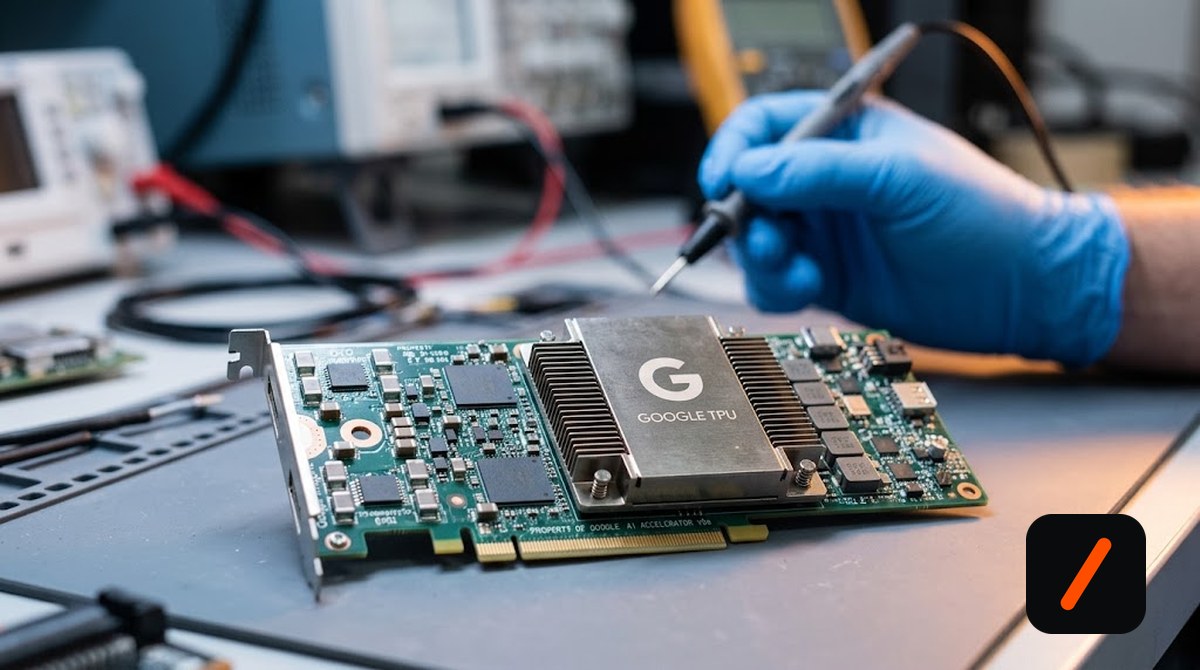
Google is designing a custom server chip that bakes Gemini directly into silicon, and the goal is blunt: run its own models far cheaper. According to a report from The Information published on July 20, 2026, the chip is known internally as Frozen v2, and Google believes it could be six to ten times more efficient than its current custom accelerators, measured by AI tokens served per unit of power. Alphabet shares rose on the report. The chip is still years away, with deployment described as possible as soon as 2028.
- Frozen v2 permanently embeds parts of the Gemini architecture into the hardware, cutting the data the chip has to shuttle around and speeding up how fast it answers a query.
- The efficiency target is 6 to 10 times the tokens per watt of Google's latest custom silicon, aimed squarely at the cost of serving models, not training them.
- It is separate from Google's TPUs, including the just-launched Ironwood generation, so it is a new hardware line rather than a TPU refresh.
- The driver is a compute capacity crunch severe enough that Google Cloud has reportedly turned away outside customers to reserve chips for its own AI workloads.
What exactly is Frozen v2?
Frozen v2 is a server chip Google is building specifically to run Gemini, and the name is a good clue to how it works. Instead of loading a model onto general-purpose hardware, the design freezes parts of Gemini's architecture into the silicon itself. The report says this reduces the amount of data the chip has to move around, which is what makes it faster at responding to queries and much cheaper to operate per answer. The headline figure is that Frozen v2 could serve six to ten times more AI tokens per unit of power than Google's latest custom AI chips.
RelatedAMD buys Taalas, betting on AI models etched into silicon
Two caveats matter before anyone treats that number as fact. First, Google has not announced the chip; this is reporting, not a product launch, and Alphabet declined to comment. Second, the timeline is long. Deployment is described as possible as soon as 2028, so even if every detail holds, this is a bet on the back half of the decade, not a chip shipping this year.
Why does baking a model into silicon save so much power?
The reason is that modern AI inference is bottlenecked by memory, not math. When a general accelerator generates a token, it has to read the model's weights out of high bandwidth memory, push them across the chip to the compute units, and do this again and again for every token in every request. Moving those bytes costs far more energy than the actual multiply-add operations, and it is the dominant reason inference is expensive at scale.
Freezing Gemini into the hardware attacks that bottleneck directly. If the weights, or large parts of them, live physically inside the chip rather than in separate memory, the distance the data travels collapses and the constant streaming largely disappears. That is where a six to ten times gain in tokens per watt could plausibly come from. The tradeoff is flexibility: a chip specialized for one model family is not something you can repurpose for the next architecture, which is exactly why this is a long-horizon internal project and not a general product.
How is this different from a TPU?
Google already designs its own AI silicon, the Tensor Processing Unit, and its seventh-generation Ironwood TPU only recently went generally available. So it is fair to ask why Frozen v2 is a separate thing. The distinction the report draws is that TPUs are programmable accelerators built to run a wide range of models, while Frozen v2 is a fixed-function part tuned for Gemini specifically. A TPU is a flexible engine; Frozen is closer to an appliance. That specialization is the whole point, and it is also the whole risk.
| Trait | Frozen v2 | Ironwood TPU | Nvidia GPU |
|---|---|---|---|
| Primary purpose | Serve Gemini only | Train and serve many models | Train and serve many models |
| Flexibility | Fixed to one model family | Programmable | Programmable |
| Where weights sit | Baked into silicon | External HBM | External HBM |
| Efficiency pitch | 6 to 10x tokens per watt | Best TPU perf per watt to date | Industry default |
| Status | Reported, unannounced | Generally available | Shipping |
| Earliest deploy | As soon as 2028 | Now | Now |
What it means for the market
Alphabet shares moved on this report for a reason: cheaper inference is the single biggest lever on AI margins, and Google runs Gemini across Search, Workspace, Android and Cloud. If Frozen v2 delivers even the low end of its claimed efficiency, Google reduces its dependence on buying expensive merchant GPUs and improves the unit economics of every AI feature it ships. The signal for investors is that Google is doubling down on owning its silicon stack, which is a structural cost advantage rivals renting Nvidia hardware do not have.
The read for Nvidia is more subtle than a knee-jerk negative. Nothing here touches near-term GPU demand, and 2028 is far away. But every hyperscaler building serious custom inference silicon chips away at the long-run assumption that all AI compute flows through Nvidia. Broadcom is the quiet name to watch: it co-designs Google's TPUs and is the main beneficiary of hyperscaler custom-silicon programs, so a new Google chip line is directionally positive for its AI ASIC business. Treat all of this as a multi-year signal, not a trade for this quarter.
RelatedNvidia Bets $3.5 Billion on MediaTek to Ride the Custom-Chip Wave
- Prior genOriginal Frozen chip developed internally Frozen v2 is the successor named in the report
- 2026Ironwood TPU v7 reaches general availability Google's flexible AI accelerator line
- Jul 20, 2026The Information reports the Frozen v2 project 6 to 10x efficiency claim, Alphabet stock rises
- As soon as 2028Possible deployment window Aimed at Google's own AI capacity crunch
Who is affected by this?
Internally, the team that feels it first is Google Cloud. The report ties Frozen v2 to a capacity crunch that has fueled tension inside the company and led Cloud to decline deals with some outside customers because chips were needed for Google's own models. A far more efficient inference chip is, in part, a way out of that squeeze. Externally, the affected group is every company weighing whether to build custom AI silicon or keep buying it. Google, Amazon and others funding in-house chips make it a little more normal, and a little more urgent, for the rest of the market to have a silicon strategy rather than a purchase order.
- Official confirmation. Google has not acknowledged Frozen v2. A mention at a Cloud or hardware event would turn a report into a roadmap.
- The efficiency claim, measured. Six to ten times is a reported target. The number that matters is what an independent workload shows, if the chip ever ships.
- Model lock-in risk. A chip frozen to today's Gemini is only valuable if Gemini's architecture stays stable enough to be worth casting in silicon.
- Broadcom's role. Watch whether Broadcom or another partner is named on the design, which would signal how real and how far along the program is.
Our take
Strip away the drama and Frozen v2 is Google admitting the same thing everyone serving models at scale has learned: inference is a memory-movement problem, and the way to win on cost is to stop moving so much data. Baking the model into the chip is an aggressive version of that idea, and if it works it is a genuine structural edge, because nobody renting general-purpose GPUs can match a chip that only has to do one job.
We would keep the excitement calibrated to the timeline. This is a report about a chip that might arrive in 2028, with an efficiency figure Google itself has not stood behind on the record, describing a design whose biggest weakness, total inflexibility, is baked in as literally as its weights are. The direction is real and it tells you where Google's head is at. The specific six-to-ten-times promise is a claim to verify later, not a fact to bank today.
- ReportingThe Information , original July 20 report on the Frozen v2 chip and its efficiency target
- ReferenceCNBC , Alphabet stock reaction and summary of the reported chip
- ReferenceBloomberg , independent write-up of the report and market context
- ReferenceGenZTech: Google's Ironwood TPU , background on Google's existing custom AI silicon
Original analysis by GenZTech. Reporting sourced from The Information via CNBC and Bloomberg.